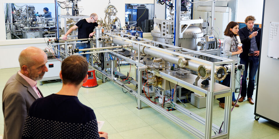
New ‘NanoAccess’ lab provides unique access to nanoworld
Making, manipulating and studying an atomic thin material, layer by layer, with nanoscale precision: NanoAccess is the only facility in the Netherlands that can offer researchers all of these possibilities at one and the same time with a single instrument. The possible applications cover a range of fields, from energy-efficient electronics to smart mobility and solar fuels. The TU/e lab officially opens its doors on Wednesday 9 November.
One of the main challenges in studying materials at nanoscale (a million times smaller than a millimeter) is that very high vacuum is required to prevent contamination and undesired reactions with the atmosphere. “NanoAccess is the only instrument in the Netherlands, and one of the very few in the world, where the vacuum does not have to be broken between the different processing steps,” says professor Bert Koopmans, TU/e researcher and project leader.
This enables not only nanoscale work to be done much more efficiently and accurately than before but also the manufacture of all kinds of new structures. “Normally it is not possible to intervene during the production process in which composite materials are constructed atomically layer by layer without breaking the vacuum,” Koopmans explains. “But now we can stack a number of layers, then etch away, add or measure with nanometer precision before continuing to stack new layers on top.”
NanoAccess comprises four clusters of vacuum chambers in which material samples can be transported fast by tubes from one cluster to the other. Each cluster has a different function with its own ‘state-of-the-art’ equipment. For example, in NanoFilm thin material films can be constructed atomic layer by atomic layer. In NanoProbe researchers are able to examine the surfaces of a material with a high degree of accuracy using a variety of analytical methods. One of the components of this is a special ‘STM’, a device for exploring a material with atomic precision that, in this case, is equipped with four independent controllable contacts. In NanoFab concentrated ion beams etch away structures in thin surfaces. NanoUser, finally, is an ‘open contact’ of the facility to which temporary specific equipment can be connected.
NanoAccess is chiefly intended for curiosity-driven research but it may also generate a wide range of possible applications. The research group of Koopmans is mainly targeting energy-efficient electronics and memory storage, using ‘spintronics’. Work also focuses on sensors for smart cars, microchips on the basis of light signals (photonics) and new materials for energy storage and solar cells, among other things.
The lab was made possible by a subsidy of nearly two million euros from the NWO Investment Grant Large program and with support from NanoLabNL. There will be significant collaboration with NXP, DIFFER and Holst in the lab. The facility will also be made available to external users such as research groups of other universities or companies. NanoAccess will be officially opened on Wednesday 9 November at 4 pm by rector magnificus Frank Baaijens and the dean of Applied Physics, Gerrit Kroesen. After the opening ceremony there will be a short guided tour of the lab.
Source: TU/e Press Team


Discussion