“We want to brand ourselves as the chip university of Europe”
TU/e intends to double the number of chip researchers and make an even bigger name for itself under the Future Chips flagship
In his new role as ambassador of the Future Chips flagship, Professor Bart Smolders wants to make sure TU/e strengthens and expands its leading position in the semicon world. “We want to show everyone, from here to South Korea, that TU/e is the place to be for anyone that wants to do anything with chips.”
“In America – and later in Europe – we have become increasingly aware that we’re too dependent on other countries that develop these technologies, such as Taiwan,” says Bart Smolders, who’s also a former Dean of the TU/e Department of Electrical Engineering. According to him, unpredictable geopolitical developments mean it’s too uncertain whether we can keep procuring chip technologies from these countries. “If something happens to Taiwan, it could have an impact on us,” he states. So his conclusion is that we have to make sure to preserve the knowledge ourselves. “That’s very important for the future, when chips will take on an increasingly important role,” says Smolders.
“Brainport is seen worldwide as one of the most important chip regions in the world, mainly owing to the strategic importance of ASML and NXP,” he continues. “As the main supplier of knowledge and engineers to these companies, we play an important role in this context as a university. Through the Future Chips initiative, we want to further strengthen and expand this leading position.”
Three pieces of the puzzle
The first steps have already been taken, by clearly mapping out everything that goes on at TU/e in the area of chips. When we talk about chips, we can distinguish three important topics. Smolders shows us a visual representation of this distinction. “First, you have the actual designing of the chips,” he explains. “These may be electronic chips, but also photonic ones – we’re very good at the latter at TU/e.” Then there are the processes and materials needed to make those chips and the equipment to apply the materials and carry out the processes. These are the three pieces of the puzzle that together make up the world of chips, from designing to making and realizing them.
All kinds of companies are involved in different areas. “This we also mapped out,” says Smolders. ASML, for instance, focuses on lithography machines that are needed to realize chips, while NXP is more involved in design. TU/e plays an important part in all of the domains relating to chips. But where all areas used to form one whole, they’ve gradually become separate disciplines. “It used to be one team, but now there are separate worlds. Interaction between researchers is limited,” he says. “They need each other, but they don’t know what the other is working on.”
For us as a university, it’s important to organize ourselves and present ourselves to the outside world as a collective
Vision of the future
One of the goals of Future Chips is to bring those worlds closer together again. “For us as a university, it’s important to organize ourselves and present ourselves to the outside world as a collective. We want to showcase everything we do, but also our ideas and our vision of the future.”
In order to determine that vision of the future, Future Chips organized sessions with the 150 scientists working on chips at TU/e and asked them: What do you think? Based on this, they defined several research vectors, i.e., areas in which various researchers are active and where they think research should be heading. "One of those is bringing together different disciplines involved in chips. This would ensure that in addition to designing a chip, you also know what kinds of materials and processes exist and what the possibilities are in terms of equipment.”
Chiplets
“We also believe that the chips as we know them today won’t exist in twenty years,” says Smolders. “Instead, you’ll see that different technologies will be physically brought together in the form of chiplets.” In chiplet architecture, different functions are placed on separate chiplets, which are then combined to form a larger, more complex chip. “Basically, two, three, four, or five chips with different functionalities are stacked on top of each other,” he explains. In so doing, each part may have been designed for a certain purpose. By combining various components and adjusting them to specific needs, manufacturers could develop chips with better performance in a much faster, more efficient, and cheaper way.
Brining together multiple technologies in one design, with each technology being optimized for a certain function, is also known as heterogeneous integration. “It’s a fundamentally different approach. We truly believe this is the future and we can play an important role in this regard, exactly because we are already active in all of those different domains,” says Smolders. “This enables us to create a better strategic position, because we can speak as a collective when we say: this is our vision. You can make a much bigger impact that way,” he feels.
The place to be
For one thing, building name recognition is important to attract new talent, as TU/e wants to double the number of chip researchers in the years ahead. “In 2030, the Dutch chip industry will need 39,000 people,” he says. “Of course, these people won’t all come from TU/e, but also from higher and secondary vocational education institutions,” he adds. That being said, it’s a pretty large number, all the more so because it excludes the people who are set to leave the industry for retirement or other reasons.
An important impetus is Project Beethoven, in which the government is to spend 2.5 billion euros on the Dutch chip sector. Out of this sum, 450 million euros are earmarked for education and talent development. This amount will be divided among various education institutions, including TU/e. At TU/e, over 700 researchers across 25 research groups are currently working on semicon (aka semiconductors or chips); in addition to around 150 permanent academic staff members, this includes around 550 PhD candidates. Thanks to the investment by the Dutch government, this number is set to increase considerably in the years ahead.
In this sense, the Netherlands isn’t a pioneer but follows a broad international trend where different countries try to reinforce their positions in the chip world, given that chips are becoming increasingly important in many important domains, such as the development and implementation of AI applications. A case in point is the adoption of the CHIPS Act by the United States Congress two years ago, making a lot of money available to the American chip industry.
We want to show everyone, from here to South Korea, that TU/e is the place to be for anyone that wants to do anything with chips, with ASML just a short bike ride away
Scaling up
There are four TU/e departments that are highly involved in semiconductors: Electrical Engineering, Mechanical Engineering, Applied Physics & Science Education, and Mathematics & Computer Science. To meet the demand for talented new hires of companies such as ASML and NXP, these four departments will have to double the number of master’s students by 2030.
“If you want to have twice the number of graduates, you’ll also need to double the number of academic staff,” Smolders observes. “This is how you get to those seven hundred extra chip researchers.” Doubling the number of researchers is, therefore, not a goal in itself, but a side effect of the higher goal: meeting industry’s growing need for qualified chip engineers. By scaling up academic staff at an equal rate, the ratio between students and staff will stay the same.
But where to get all of those new researchers? “That’s a very good question,” Smolders responds. “In recent years, our university grew considerably, so we obviously have a good number of talented PhD candidates in the pipeline. That’s one. It goes without saying we’ll also have to attract people from outside the Netherlands. That’s why we want to show everyone, from here to South Korea, that TU/e is the place to be for anyone that wants to do anything with chips, with ASML just a short bike ride away.”
Closer collaboration
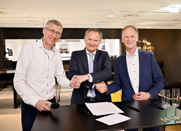
On May 23, TU/e and ASML signed an agreement on the expansion of their collaboration. The closer collaboration means that in the decade ahead, “almost a hundred PhD students” will be doing research on areas “relevant to the chip sector” on the TU/e campus. Smolders doesn’t see the increasingly close ties with industry as a problem. On the contrary, he considers it a necessity. “As a university you have to work together with industry, otherwise you’re a nobody. Then you can forget about playing any kind of role in the world of chips,” he argues.
A company like ASML benefits from a university that goes against the grain a little bit and dares to explore different paths
It’s exactly because we are close to industry and many of our alumni work at companies such as ASML that we have very warm contacts and that it’s easier for us to work together well with industry, he says. “But it’s still our own roadmap,” he emphasizes. That is also why the flagship was set up as a completely internal initiative, without involving the industry. “It concerns our own vision of the future, topics we ourselves attach importance to. Of course we know what industry wants. But it’s a bottom-up process in the end.”
He doesn’t deny that ASML expresses a clear interest in concrete solutions to its issues, but it’s the university itself that ultimately determines the focus of the research. “A company like ASML actually wants us to have a strong vision as well,” says Smolders. “Right now, they focus on current problems, but they also want to know what to do in ten or twenty years from now. Maybe by then you’ll need an entirely different machine or different competencies. So then a company like ASML also benefits from a university that goes against the grain a little bit and dares to explore different paths.”
New cleanroom
Part of the agreement with ASML is the realization of a new cleanroom on the TU/e campus by 2026, alongside the existing one. “It will be at least 50% bigger and will include a section – and this I’m super excited about – where students can work,” says Smolders. Whereas the current cleanroom is solely intended for research, in future it will be possible to use the new one for education purposes as well. This will allow students to familiarize themselves with the world of chips even before they graduate.
It would be ideal for students if they could first design their own chips using software, then go into the cleanroom to use real machines to make the chips, and then assess the chips and test if everything is working. “This is how we’ll bring the design, manufacturing, and equipment together, showing how the entire process works,” says Smolders. This will allow TU/e to set itself apart, because it’s not typical for students to be allowed to work in such a lab. After all, the equipment is generally very expensive and people are afraid that students who don’t know how everything works will cause chaos. “We want to create a controlled environment where the students can explore everything themselves while under supervision,” says Smolders. The room will be deliberately set up in such a way that it’s okay if something goes wrong. “It’s all about making mistakes and experiencing firsthand why something isn’t working. That teaches you the most.”
Chips in a nutshell
What are chips?
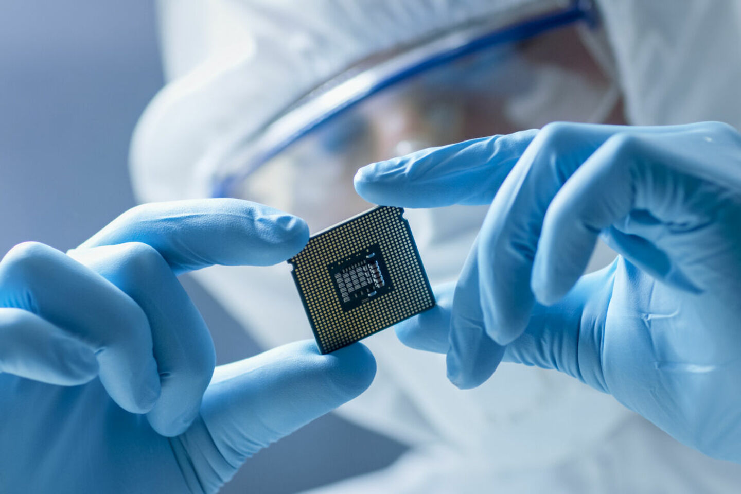
Chips are small pieces of silicon containing complex electronic circuits. They perform important tasks in electronic devices, such as calculation in computers and smartphones, data storage in memory cards and SSDs, and coordination of functions in machines such as televisions, cars, and household appliances. You could see them as the ‘brains’ of modern electronics, making sure that devices operate correctly.
How are chips made?
Smolders shows us a thin plate. “This is what you see when you crack open an iPhone, for instance,” he explains. What is known as the Printed Circuit Board – PCB for short – is an essential part of devices such as smartphones and computers. He points out the small black cubes on the plate – these are the chips. In addition to chips, the PBC also contains other electronic components that are crucial to the workings of modern electronics.
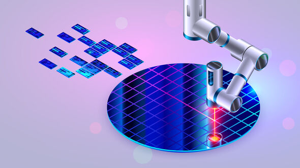
The chips on the PCB are made of ‘wafers’, thin disks of semiconducting material, typically silicon. After the silicon has been cut into these disks, they are equipped with small electronic circuits (also known as integrated circuits or ICs). The disk is then cut into little pieces – each piece is a chip. These chips are subsequently packaged in plastic and placed on a PCB, after which they’re secured and mounted into the electronic device concerned.
What does the production process look like?
The production process starts out by designing the chip with special software on the computer, determining such things as the number of transistors. Then comes the lay-out, a kind of blueprint containing details such as the location of metal traces and transistors. This blueprint is sent to a factory for chip production, typically located in countries like Taiwan. There, the wafers are produced according to the specifications of Apple, NXP, and other companies. The wafers are then sent to another factory, often in countries like the Philippines and China, where they’re cut and packaged.


Discussion